
Q&A: From Components to Complete Optical Subsystems: The Novanta and Optikos Collaboration
Date
July 22, 2026
Author
Daniela Dandes
Time
6 min
Share this Post
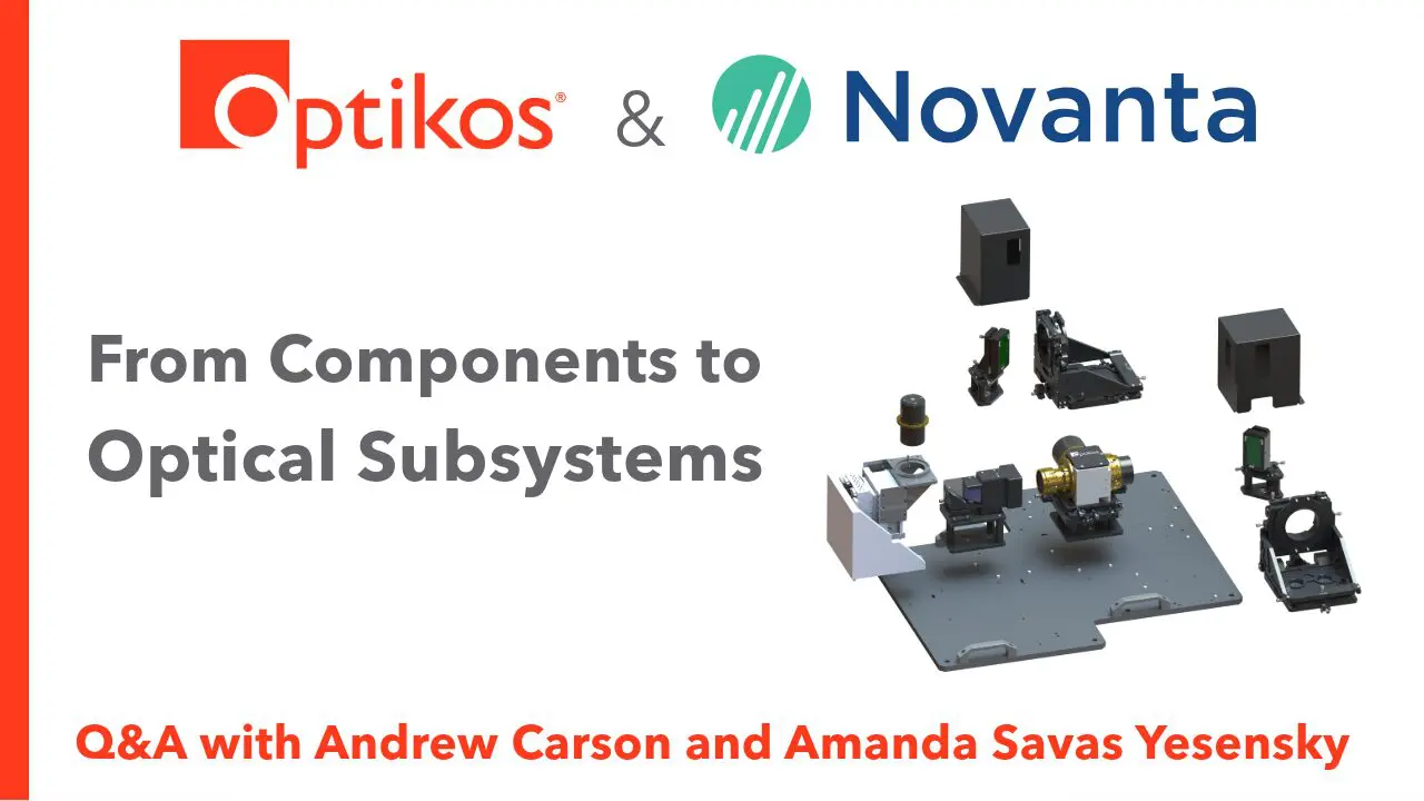
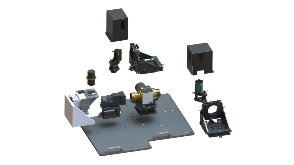
For years, life science innovators have been faced with the challenge of choosing between high-performance optical imaging and cost-effective scalability. Novanta is changing that paradigm with a purpose-built, multi-channel fluorescence imaging platform engineered to accelerate the path from concept to proof-of-concept. By combining optimized optics, highly tuned sample positioning, modular architecture elements and application-focused design, the system delivers high-quality data from day one, enabling faster development cycles and improving the accuracy and reliability of image analysis. To bring this vision to life, Novanta partnered with Optikos to develop the advanced optical imaging subsystem that is at the heart of the platform, ensuring uncompromising performance, flexibility, and value in a solution designed for next-generation scientific discovery.
We caught up with Andrew Carson, Senior Director of Engineered Systems, and Amanda Savas Yesensky, Senior Director of Global Sales at Novanta, to explore how purpose-built, configurable optical system design is helping life science innovators accelerate the path from concept to proof-of-concept. In this conversation, they share how an application-focused modular design approach brings instrumentation developers closer to delivering the “clearest pixels” to their customers in labs worldwide.
Q: Hey Andrew, hi, Amanda, thank you for making time for this interview. It’s an exciting moment to be involved in the optics industry.
Amanda Savas Yesensky (ASY): Hello, it definitely is.
Andrew Carson (AC): Hi, I completely agree. It’s really an exciting time.
Q: Let’s talk about your starting point with this new capability that Novanta is sharing with life science tool makers. Novanta has built its reputation around enabling innovation through precision photonics, configurable illumination subsystems, and motion technologies within medtech and advanced industrial applications. What inspired your team to focus on the new dual channel fluorescence optical imaging system?
ASY: That’s a great question, and honestly, it’s one we challenged ourselves with early on. The fluorescence instrumentation market certainly isn’t lacking options, but when we spoke with researchers, instrument developers, and emerging life science companies, we saw a consistent need: getting high-quality answers faster, with less complexity, lower development risk, and more efficient use of both time and resources.
AC: We took that voice of customer and translated it into a configurable multichannel fluorescence imaging platform. The intent was to create an architecture that can be used as a rapid development tool, adapting to customers’ assay requirements, optical configurations, and system-level workflows to allow for practical test and development before locking in specs. That flexibility matters because it allows researchers and instrument developers to accelerate decision-making, whether they are proving a concept for funding, evaluating assay viability, or moving a new technology toward commercialization. Faster time-to-answer means more efficient use of engineering and laboratory resources, lower development cost, and ultimately a faster path to market.
ASY: What I’d add to that is the fact that Novanta brings deep expertise in illumination, motion control, and system integration. By combining these capabilities with the Optikos optical imaging expertise, we were able to create a fully integrated, source-to-sample-to-sensor solution that will help customers achieve high-performance imaging without the burden of piecing together and optimizing multiple technologies themselves. What we saw was a need for a more integrated, optimized system that helps users move from idea to answers faster and more efficiently.
Q: How did Optikos stand out as a partner-of-choice in this project?
ASY: Novanta was looking for a partner with proven imaging system design and volume manufacturing expertise, capable of operating at the system level rather than as a component supplier. The ideal company needed to have the ability to translate application-level requirements into robust optical imaging designs, support manufacturability and scalability, and engage in deep, engineer-to-engineer co-development. Optikos brought the right combination of technical depth and commercial maturity. The team has deep expertise in optical design and imaging systems, and they also understand bringing a product to market in practice.

“What stood out to me in particular was how quickly the Optikos team connected the application requirements to the optical design approach. The people we worked with were able to take a high-level system objective and translate it into detailed performance requirements, engineering trade-offs, and design decisions required to make the whole architecture work.”
Beyond the technical capability, there was a strong operating fit. We had a similar engineering mindset by defining the problem clearly, making the right trade-offs, managing risk, and keeping the program aligned to the system-level objective. They also knew how to execute what was discussed. From technical leadership through the broader engineering team, Optikos delivered predictable progress, which is exactly what you need on a complex development program.
Q: What did the beginning of the collaboration look like?
ASY: The beginning of the collaboration was all about aligning on what would truly drive performance. We had a clear vision for the system—translating that into the right specifications and design choices required optical expertise and a solid understanding of the application.
One of the biggest challenges was identifying the parameters that mattered most and understanding the trade-offs involved. Optikos helped accelerate that process by sharing early concepts and models, which made the discussions much more concrete and data-driven.
That transparency allowed us to align quickly on a practical, high-performance, configurable design. As a result, we were able to move efficiently from concept to a manufacturable solution, with confidence that we were optimizing for both performance and usability.
Q: How does the new imaging subsystem design fit in with your team’s vision for the full optical platform?

“The subsystem design delivered exactly what we set out to achieve. It met the optical performance requirements while providing the modularity and scalability needed to support future platform evolution. That was important because our vision wasn’t just to develop a single instrument; it was to create a flexible platform that delivers long-term value through improved performance, lower development costs, and greater reuse across applications.”
The collaboration also played a significant role for the outcome. We established a consistent operating rhythm with weekly reviews, direct engineer-to-engineer engagement, and clear milestone tracking. That level of alignment helped us make decisions quickly, manage risk proactively, and keep the program moving efficiently as requirements evolved.
Q; What specific technical advantages does this platform offer regarding image quality and integration time?
AC: The teams used a holistic, systems engineering approach to balance the design requirements of critical subsystems and components to deliver diffraction limited performance across the field of view (FOV), while maintaining scalability to allow for rapid development across a broad range of applications. The main advantage is that this approach produced an engineered optical imaging platform, not a set of discrete components that would have to be integrated individually—the system came together in days, rather than weeks. The optical path, illumination, motion, controls, and imaging chain were designed to work as one system, so we solved the integration problem right at the beginning of the program. This translates to a platform that can be configured, scaled, and adapted quickly to customers’ varying applications.
By achieving high image quality across a large field, we enabled rapid integration time, while also reducing the amount of alignment, tuning, and validation work required. For instrument developers, every week spent integrating subsystems is a week not spent generating data, proving the application, or moving toward a customer-ready platform. With our platform we can reduce that burden, lower development risk, shorten time-to-answer, and give customers a more practical path from concept to a deployable system.
Q: So, everyone in this field should be very excited for this new capability?
AC: We certainly are. We believe it has the potential to help researchers and instrument developers accelerate progress by reducing complexity and getting to meaningful results faster.
Q: Thank you, Amanda and Andy, for sharing the story behind Novanta’s multi-channel fluorescence optical imaging platform. On the Optikos side, I know it’s our pleasure to work with your team on such a relevant product.
ASY: Likewise. It’s been a great partnership, and we’re excited to see what our customers and the broader scientific community can achieve with this platform.
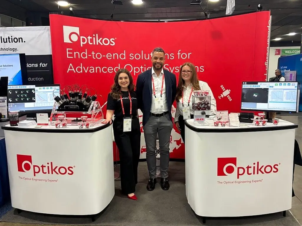
Interested in learning more? Discover how the Novanta and Optikos dual-channel fluorescence imaging system can help accelerate your path from concept to insight. Connect with our teams to schedule a discussion, or visit the Optikos booth #1560 at ADLM 2026, July 26–30 in Anaheim, California, to see the system in action.
Author Bio

Share this Post
See More Posts
Blog
Heuristics Are Making Way for Hard Data in the Nightforce Optics and Optikos Partnership
09/25/2026
•
6 min

Blog
Optikos Achieves Zero-Finding
ISO 13485 Recertification: A Conversation with Nick Mastrocola, Quality Manager at Optikos
07/13/2026
•
6 min
Blog
Advancing Automotive Imaging and Thermal Testing Insights from AutoSens USA 2026
06/24/2026
•
5 min