
Whoops! This page slipped beyond our depth of field.
Let's bring your search back in focus ↓
This page may have scattered—but our fresh content is perfectly collimated. Explore below:
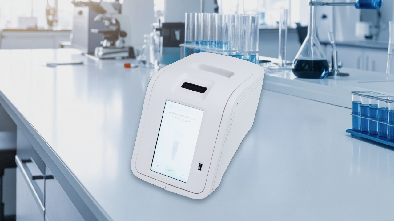
From Clean Sheet Design to Operational Proof-of-Concept
Optikos rapidly transformed a fragile breadboard DNA/RNA detection concept into 15 reliable, long‑lasting demonstrator units. Using a gated medical‑device development process, multidisciplinary engineering, and strategic partnerships, Optikos delivered a robust optical detection platform that continues to support ongoing R&D years later.
Read the Study
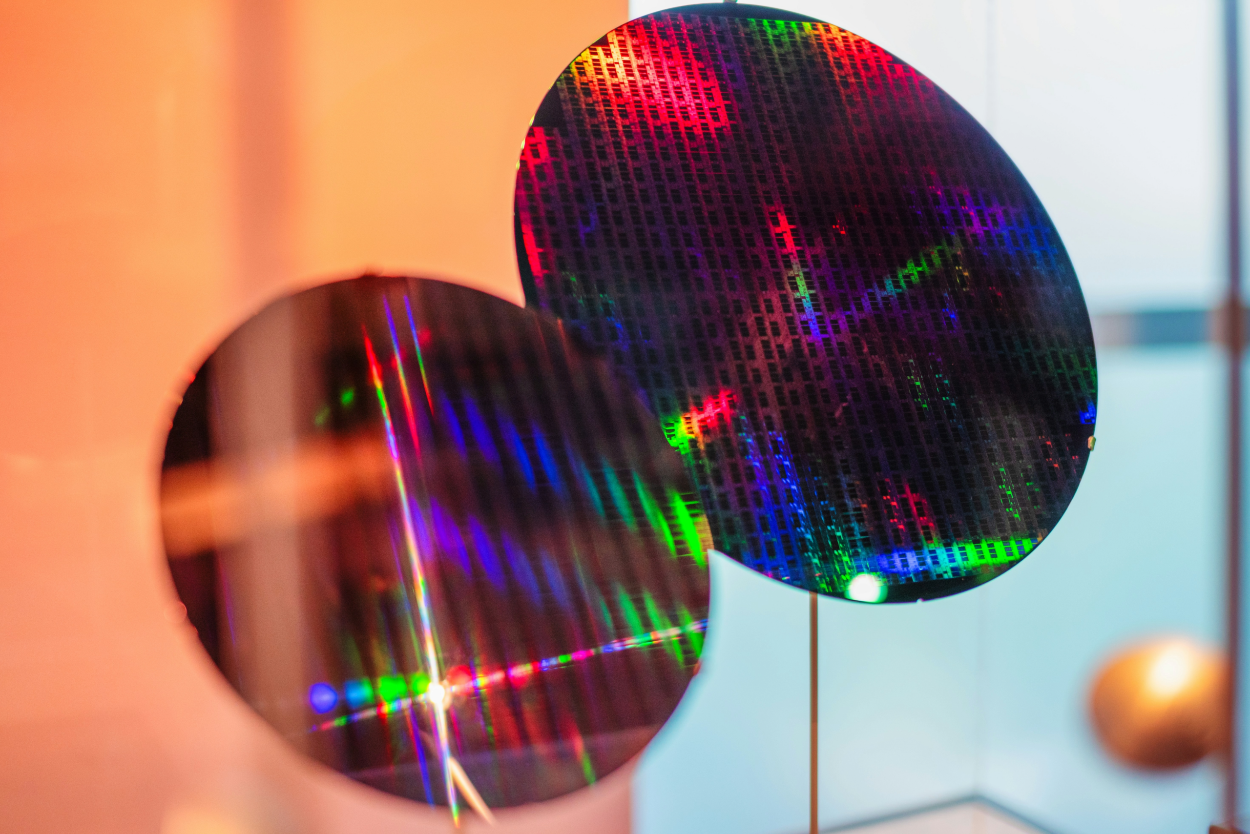
Optikos Enables Next‑Generation Wafer‑Overlay Metrology Platform
Optikos designed and manufactured a custom wafer overlay imaging module featuring sub‑micron repeatability, metrology‑grade stability, and complete optical and mechanical IP ownership.
Read the Study
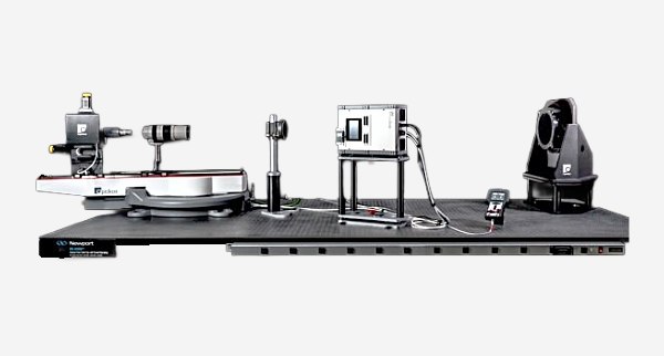
Giving Stray Light a Home
Optikos identified and eliminated a critical stray light issue by combining advanced Zemax modeling, precision metrology, and targeted opto‑mechanical redesign—achieving over 10× reduction in unwanted reflections.
Read the Study
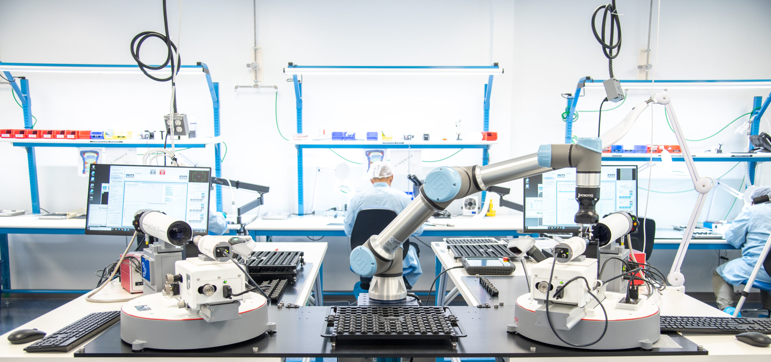
Automation Strategy Cuts Cycle Time by 50% for AR Lens Testing
View/print as a PDF Primary Challenges & Breakthroughs Overview The world of lens manufacturing is ruled by three important production parameters: quality, investment, and time. Within this matrix, the testing phase of optical systems is paramount because of the “zero-tolerance for defects” nature of the sector. What garners criticality around this phase of the manufacturing process is the rapid growth
Read the Study