
From “Black Box” Risk to Full Design Ownership
Key Achievements:
Time to market accelerated – qualified production quantity modules arrived ready to integrate, dramatically cutting integration lead time.
100% design ownership restored – the client now holds the complete optical and mechanical IP and can approve any future change to the optical solution.
100% supply chain risk eliminated – a custom, documented module removed the end of life surprise that threatened the product line.
Summary
- Problem: Uncontrolled revisions of off the shelf imaging modules for wafer inspection line created variability, re qualification effort, and an EOL (end-of-life) supply chain threat.
- Solution: Optikos delivered a fully custom, metrology qualified imaging module designed, built, and transferred to the customer under strict change control.
- Result: The client now enjoys stable optical performance, repeatable production, and strategic control of a critical subsystem for their wafer overlay tools.
The Customer
A US based supplier of high end semiconductor capital equipment chose Optikos for their unique manufacturing requirements. Their portfolio includes sensor based systems, software analytics, and integrated platforms designed to improve quality control, process efficiency, and predictive maintenance. This company’s semiconductor metrology tools enable device and substrate manufacturers to boost yield, reduce variability, and speed up production ramps for AI, high performance computing, and heterogeneous/advanced packaging workloads.
Industry: Semiconductor · Wafer Overlay Metrology
The Problem
The client relied on a suite of optical and macro defect inspection instruments to deliver the precision needed for demanding applications within semiconductor manufacturing. However, the imaging module at the heart of their next generation wafer overlay system was sourced from an off the shelf catalog. Over successive tool generations, the commercial vendor altered the design several times. Each revision introduced subtle optical shifts that forced the client to pause production for requalification. When their vendor announced the end of life (EOL) of the commercial part, the client faced a looming supply chain gap that threatened the continuity of a high value metrology platform. Lacking a documented, customer owned design, they had no straightforward path to replace or modify the module without incurring extensive downtime and engineering effort.
The multi-faceted challenge included:
- Legacy reliance on off the shelf imaging modules that were revised repeatedly by the original supplier, introducing optical variability and forcing costly requalification campaigns.
- End of life (EOL) of the commercial module created a severe supply chain risk for a high value metrology product line.
- Overlay metrology demands extremely stable, well characterized optics; any unplanned module change triggers downtime and requalification.
- The customer needed a controlled, documented, fully transferable design that they could own and manage throughout the tool’s long lifecycle.
Our success criteria: Optikos needed to meet/exceed precision optical performance, mechanical compatibility, repeatable production, and volume ready manufacturing without compromising optics.
“Optikos provided additional value by manufacturing the imaging module in production quantities for the customer, reducing lead‑time and delivering a qualified module for integration into their system.”
– Dennis Fantone, Director of Operations at Optikos
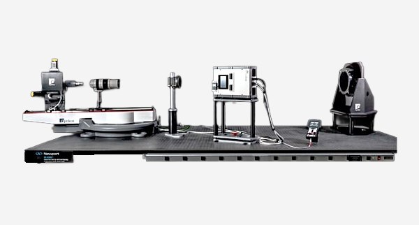
How Optikos Solved this Problem
[Requirements]→[Custom Optical + Mechanical Design]→[via Metrology First Qualification]→[Production Build]→[Delivery & Integration]
- Requirements and Interface Definition: The Optikos engineers began by working closely with the client to capture every optical performance metric, detector and interface specification, and environmental constraint. At the same time, the team verified the mechanical envelope of the existing wafer overlay system, ensuring that the new module would fit perfectly without any redesign of the surrounding hardware.
- Custom Imaging Module Design: Rather than adapting an off the shelf part, Optikos engineered a wholly bespoke optical and opto-mechanical assembly. The design prioritized absolute stability, ease of manufacture, and long term configuration control, guaranteeing that the module would remain consistent across production runs and over the tool’s lifespan.
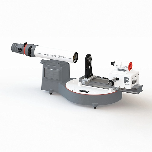
- Qualification for Client Specs: Leveraging our metrology first philosophy, our teams not only designed the module but also qualified it against the client’s stringent specifications. By embedding rigorous metrological testing into the development flow, the company dramatically reduced the re qualification effort the client would otherwise have faced.
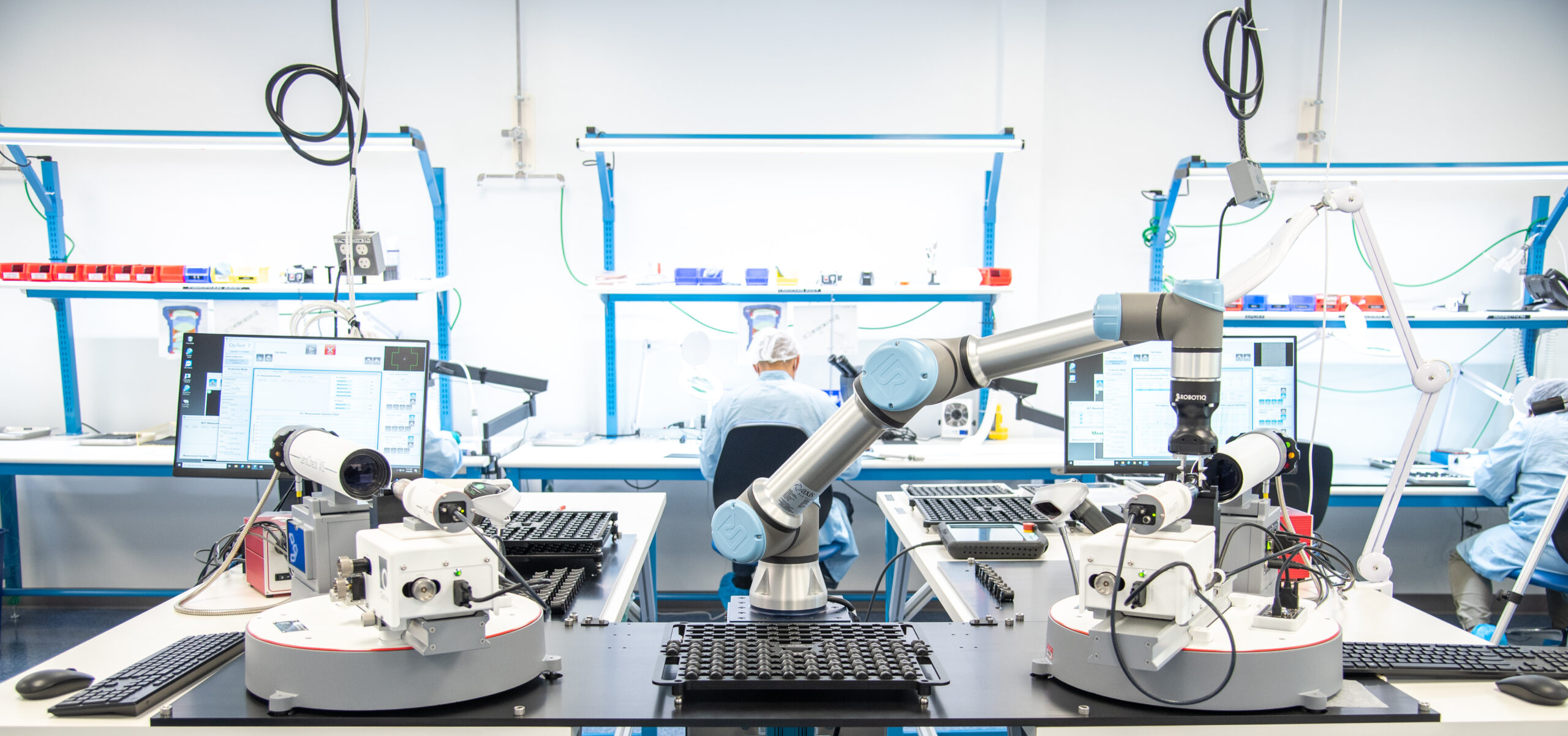
- Transition to Production: Once the design received formal acceptance, the assembly moved straight into volume manufacturing. The imaging modules were produced in the required quantities, each unit fully qualified and ready for immediate integration. This process shortened lead times and delivered a plug and play solution for the client’s next generation wafer overlay system.
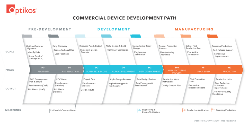
This development process aligns with the Optikos Commercial Development Path which has been validated across thousands of past product designs.
“The biggest accomplishment is that the assembly is robust, has a high degree of up time and the mechanisms feature a level mechanical precision that is very challenging to achieve.”
– Nathan Wallace, Director of Engineering Services at Optikos
Achieving Precision Engineered Stability
Optikos’ hallmark is its rigorous mechanical repeatability program, engineered with a strong design for manufacturability focus. Every moving component within the imaging module is subjected to extensive cyclic testing, during which positional accuracy is repeatedly verified under controlled, repeatable conditions. This test regime consistently achieves sub-micron repeatability, demonstrating that the module retains precise alignment and performance through thousands of insertions, thermal cycles, and vibration events. The resulting data are incorporated into the module’s qualification package, providing clients with documented assurance that the optics will remain accurately calibrated throughout the instrument’s service life.
Conclusion
Optikos transformed a risky, off the shelf dependency into a strategic asset for the semiconductor OEM:
- Design ownership now resides with the customer, eliminating hidden supplier changes.
- Supply chain resilience is restored, removing the EOL threat.
- Integration speed improved thanks to qualified, volume ready modules.
- Long term configuration control enables future upgrades under a formal change control process.

Key Takeaways for Semiconductor / Metrology OEMs
Optikos transformed a risky, off the shelf dependency into a strategic asset for the semiconductor OEM:
- Own the design of any imaging module that directly impacts metrology performance.
- Partner with a provider capable of custom design, qualification, and volume manufacturing—not just catalog parts.
- The Optikos end to end expertise (engineering services, manufacturing, metrology) makes a partnership uniquely suited for long lifecycle, high precision tools.