
Published
December 3, 2013
ABSTRACT
An intgeral printhead includes a single fiber optic faceplate substrate to which are connected light emitting diode arrays, driver circuits for selectively controlling the energization of the light emitting diodes and interconnecting conductive lines all disposed on the same fiber optic faceplate substrate which thereby provides the optical lens system for the light emitting diodes and a supporting substrate to which the active components are mounted and electrically interconnected by the conductive lines.
| Publication number | US4921316 A |
| Publication type | Grant |
| Application number | US 07/319,612 |
| Publication date | May 1, 1990 |
| Filing date | Mar 6, 1989 |
| Priority date | Mar 6, 1989 |
| Fee status | Paid |
| Also published as | CA2008748A1, EP0402341A1 |
| Inventors | Robert J. Burger, Lee M. Cook, Stephen D. Fantone, Bennett H. Rockney |
| Original Assignee | Galileo Electro-Optics Corporation, Polaroid Corporation |
| Patent Citations (14), Non-Patent Citations (4), Referenced by (8),Classifications (10), Legal Events (16) | |
| External Links: USPTO, USPTO Assignment, Espacenet | |
DESCRIPTION
BACKGROUND OF THE INVENTION1. Field of the Invention
This invention relates generally to an integral fiber optic printhead and, more particularly, to a printhead comprising a single fiber optic faceplate substrate.
2. Description of the Prior Art
Light emitting diode arrays are well known in the art for recording an image on a photosensitive medium such as a photographic film or paper or, alternatively, a photocopying receptor such as a selenium drum or a zinc oxide paper. In order to achieve high resolution, a large number of light emitting diodes are arranged in a linear array and means are included for providing a relative movement between the linear array and the photosensitive medium so as to effect a scanning movement of the linear array over the surface of the photosensitive medium. Thus, the photosensitive medium may be exposed to provide a desired image one line at a time as the LED array is advanced relative to the photosensitive medium either continuously or in a stopping motion. Each LED in the linear array is used to expose a corresponding pixel in the photosensitive medium to a value determined by image defining electronic signal information. Since the light emitted from each LED rapidly diverges upon emission from the diode, an optical system is needed to transmit the light from the LED to the surface of the photosensitive medium without substantial divergence. One such proposed optical system for use in such a printhead comprises an array of graded index lenses made up of closely packed rows of optical fibers as disclosed in U.S. Pat. No. 4,447,126, entitled “Uniformly Intense Imaging by Close Packed Lens Array”, by P. Heidrich et al., issued May 8, 1984. Another apparatus disclosed for mounting an imaging lens array formed of a plurality of gradient index optical fibers onto a printhead having a linear array of light emitting diodes is suggested by U.S. Pat. No. 4,715,682, entitled “Mount for Imaging Lens Array on Optical Printhead”, by K. Koek et al., issued Dec. 29, 1987. Although arrays of gradient index optical fibers have been suggested for use as the imaging lens in such printheads, critical alignment and assembly problems still exist so as to effect the precise connection between the optical fiber array and the LED array. Not only must the LED arrays be precisely aligned to the optical fiber arrays but electrical connections must also be made from remotely stationed control circuits which modulate the current furnished to drive the LED’s during exposure.
Therefore, it is a primary object of this invention to provide an integral printhead structure in which LED arrays and the driver circuits therefor can be mounted on a singular substrate.
It is a further object of this invention to provide an integral printhead structure in which light emitting diode arrays are more easily connected to a fiber optic lens array which can further act as a substrate to accommodate the mounting and connection of additional support circuitry.
Other objects of the invention will be in part obvious and will in part appear hereinafter. The invention accordingly comprises a structure and system possessing the construction, combination of elements and arrangement of parts which are exemplified in the following detailed disclosure.
SUMMARY OF THE INVENTIONApparatus for selectively exposing a plurality of longitudinally spaced areas across the face of a photosensitive medium comprises an elongated coherent fiber optic faceplate substrate. The fiber optic faceplate has a substantially planar light receiving surface oppositely spaced apart with respect to a substantially planar light emitting surface. The light emitting surface is stationed to accommodate the close proximity placement of the photosensitive medium to receive the light emitted therefrom. There is also provided at least one elongated array comprising a plurality of light emitting diodes. Each of the light emitting diodes is closely spaced with respect to an adjacent diode and has a light emitting surface fixedly stationed in close light transmitting proximity to the light receiving surface of the fiber optic faceplate. Conductive interconnecting lines are selectively deposited on the light receiving surface of the fiber optic faceplate to accommodate select electrical connection to the light emitting diodes. Means are also provided for electrically connecting the light emitting diodes to select ones of the conductive interconnecting lines. There are also preferably provided a plurality of drive control circuits for controlling the energization of the light emitting diodes. The drive control circuits are also fixedly stationed with respect to the light receiving surface of the fiber optic faceplate in spaced relation with respect to the light emitting diodes. There are also provided means for electrically connecting the driver control circuits to select ones of the conductive interconnecting lines. In the preferred embodiment, the means for electrically connecting the light emitting diodes and the driver control circuits to selected ones of the conductive interconnecting lines comprises connections made by the so-called flip chip/solder bumping process.
DESCRIPTION OF THE DRAWINGSThe novel features that are considered characteristic of the invention are set forth with particularity in the appended claims. The invention itself, however, both as to its organization and its method of operation, together with other objects and advantages thereof will be best understood from the following description of the illustrated embodiment when read in conjunction with the accompanying drawings wherein:
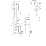
FIG. 1 is a plan view of the integral fiber optic printhead of this invention;
FIG. 2 is a cross-sectional view taken across the lines 2–2 of FIG. 1; and
FIG. 3 is an enlarged cross-sectional view showing a portion of the integral fiber optic printhead of FIG. 1.
DESCRIPTION OF THE PREFERRED EMBODIMENTReferring now to FIGS. 1-3, there is shown at 10 the printhead assembly of this invention comprising a fiber optic faceplate 12. The fiber optic faceplate 12 is configured in an elongated parallelepiped shape having a substantially planar light receiving surface 14 in spaced parallel relation to a substantially planar light emitting surface 16. The fiber optic faceplate comprises a plurality of individual glass fibers which are stacked together, pressed and heated under pressure to form a uniform structure with a plurality of light transmitting passages extending between the light receiving and light emitting surfaces 14, 16. Fiber optic faceplates are well known in the art as taught in U.S. Pat. No. 4,179,596, entitled “Method For Processing Fiber Optic Electronic Components of Electronic Vacuum Device”, by C. Bjork, issued Dec. 18, 1979, and now incorporated by reference herein. The above-described method is only exemplary, and it will be readily understood that other methods may also be utilized.
Disposed on the light receiving surface 14 of the fiber optic faceplate 12 are three elongated arrays 18, 20 and 22 comprising, respectively, pluralities of light emitting diodes (LED’s) 24, 26 and 28 aligned in side-by-side relationship with respect to each other along the length of each respective array. Each of the LED’s 24, 26 and 28 is preferably selected to emit radiation in one of three distinct wavelength ranges as for example red, blue and green. As will be well understood, other wavelength ranges could also be utilized. The LED’s 24, 26 and 28 are of conventional construction well known in the art. A plurality of LED driver circuits 32 are also mounted on the light receiving surface 14 of the fiber optic faceplate 12. Driver circuits 32 are electrically connected to select ones of the LED’s 24, 26 and 28 by means of conductive interconnecting lines 40. The conductive interconnecting lines 40 may comprise any suitably conductive metal such as gold, aluminum, etc. deposited on the light receiving surface 14 of the fiber optic faceplate 12 by any well-known technique such as sputtering or evaporation with the excess metallization being thereafter removed by well-known photoresist and etching techniques to provide selective interconnects between the LED’s 24, 26 and 28 and respective ones of the driver circuits 32.
Referring specifically to FIG. 3, there is shown an enlarged cross-sectional view of one of the LED’s 24. Light emitting diode 24 has metallized contacts as shown at 38 deposited in any well-known manner and a narrow central light emitting area as shown generally at 34. The metallized contacts 38 are electrically connected to respective ones of the conductors 40 by a conventional solder bumping process. The driver circuits 32 can be interconnected to respective ones of the conductors 40 by the same solder bumping process used to connect the LED’s or by conventional wire bonding techniques. Since the electrical connections to the fiber optic faceplate substrate 12 are made on the underlying surface of the active elements, the connection technique is generally referred to as the flip chip/solder bumping process. Although the flip chip/solder bumping process is preferred for connecting the active components to selective conductors 40 on the fiber optic faceplate substrate 12, the invention is by no means so limited and other conventional techniques such as wire bonding may also be utilized.
During the operation of the printhead 10 of this invention, a photosensitive sheet 30 is moved relative to the light emitting surface 16 of the fiber optic faceplate substrate 12 to effect a raster line exposure thereof. The radiant energy emitted by the light emitting area of each diode 34 diverges slightly in the space 42 between the underlying surface of the light emitting area and the light receiving surface 14 of the fiber optic faceplate 12. Once incident to the light receiving surface 14 radiation is transmitted in a collimated beam 44 by the fused glass fibers of the fiber optic faceplate 12 until exiting from the light emitting surface 16 to expose the photosensitive sheet 30. As will be readily understood, the radiation emitted by the light emitting diodes 24, 26 and 28 are all transmitted in collimated beams 44 without substantial divergence by respective ones of the diffused optical fibers of the faceplate 12 to expose discrete pixel areas on the photosensitive sheet 30. Transmission of the radiation from the light emitting diodes without substantial divergence operates to contain the size of the discrete areas exposed on the photosensitive so that the resolution of the reproduced image is substantially determined by the size and spacing of the LED’s 24. The driver circuits 32 operate to control or modulate the flow of current through respective ones of the LED’s 24, 26 and 28 in a manner as is fully described in U.S. Pat. No. 4,525,729, entitled “Parallel LED Exposure Control System”, by M. Agulnek et al., issued June 25, 1985, and now incorporated in its entirety by reference herein.
Thus, there is provided a simple and economical construction in which a single fiber optic substrate operates to transmit light from light emitting diode arrays in collimated beams to expose well-defined pixel areas of a photosensitive sheet while simultaneously providing a substrate onto which other conductors and LED driver circuitry may be deposited by standard techniques.
Other embodiments of the invention including additions, subtractions, deletions, and other modifications of the preferred disclosed embodiments of the invention will be obvious to those skilled in the art and are within the scope of the following claims.
CLAIMS(5)
What is claimed is:
1. Apparatus for selectively exposing a plurality of longitudinally spaced areas across the face of a photosensitive medium comprising:
an elongated coherent fiber optic faceplate substrate having a substantially planar light receiving surface oppositely spaced apart with respect to a substantially planar light emitting surface, said light emitting surface being stationed to accommodate the placement of the photosensitive medium in sufficiently close proximity thereto so that the photosensitive medium can receive the light emitted from said light emitting surface;
at least one elongated array comprising a plurality of light emitting diodes each of said light emitting diodes being selectively spaced with respect to an adjacent diode and having a light emitting surface fixedly stationed in effective light transmitting relation to the light receiving surface of said fiber optic faceplate;
conductive interconnecting lines selectively deposited on the light receiving surface of said fiber optic faceplate in a manner whereby said conductive interconnecting lines accommodate select electrical connection to said light emitting diodes; and
means for electrically connecting said light emitting diodes to selected ones of said conductive interconnecting lines.
2. The apparatus of claim 1 further comprising a plurality of driver control circuits for controlling energization of said light emitting diodes, said driver control circuits being fixedly connected with respect to the light receiving surface of said fiber optic faceplate in spaced relation with respect to said light emitting diodes, by means for electrically connecting said driver control circuits to selected ones of said conductive interconnecting lines.
3. The apparatus of claim 2 wherein said means for electrically connecting said light emitting diodes and said driver control circuits to selected ones of said conductive interconnecting lines comprises connections made by the flip chip bonding process.
4. The apparatus of claim 3 comprising at least three elongated arrays of light emitting diodes each of said arrays aligned in substantially parallel spaced relation with respect to each other and capable of emitting radiation in one of three distinct wavelength ranges.
5. The apparatus of claim 2 wherein said fiber optic faceplate comprises a plurality of solid glass fibers extending longitudinally between said light receiving surface and said light emitting surface bonded together in a fused matrix.
PATENT CITATIONS
| Cited Patent | Filing date | Publication date | Applicant | Title |
|---|---|---|---|---|
| US4179596 * | Apr 27, 1978 | Dec 18, 1979 | Litton Systems, Inc. | Method for processing fiberoptic electronic components of electronic vacuum devices |
| US4279483 * | Mar 18, 1980 | Jul 21, 1981 | The Monotype Corporation Limited | Electro-optical character generator for photocomposing apparatus |
| US4447126 * | Jul 2, 1982 | May 8, 1984 | International Business Machines Corporation | Uniformly intense imaging by close-packed lens array |
| US4482214 * | May 12, 1982 | Nov 13, 1984 | U.S. Philips Corporation | Device for applying light to a linear array of magneto-optical light switches, notably for optical printers |
| US4525729 * | Apr 4, 1983 | Jun 25, 1985 | Polaroid Corporation | Parallel LED exposure control system |
| US4574317 * | Dec 12, 1983 | Mar 4, 1986 | Wayne Scheible | Hand scannable portable copier and method |
| US4589732 * | Dec 23, 1982 | May 20, 1986 | Seiko Epson Corporation | Liquid crystal optical printing apparatus with rod lens |
| US4590492 * | Jun 7, 1983 | May 20, 1986 | The United States Of America As Represented By The Secretary Of The Air Force | High resolution optical fiber print head |
| US4715682 * | Jul 11, 1986 | Dec 29, 1987 | Eastman Kodak Company | Mount for imaging lens array on optical print head |
| US4740803 * | Jun 25, 1987 | Apr 26, 1988 | Eastman Kodak Company | Photo imaging system using two-dimensional optical lens array |
| US4750799 * | Jul 10, 1985 | Jun 14, 1988 | Nippon Telegraph And Telephone Corporation | Hybrid optical integrated circuit |
| US4752806 * | Jun 23, 1986 | Jun 21, 1988 | Xerox Corporation | Multi-mode imaging system |
| US4767172 * | Mar 11, 1985 | Aug 30, 1988 | Xerox Corporation | Collector for an LED array |
| US4837587 * | Dec 31, 1987 | Jun 6, 1989 | Eastman Kodak Company | Non-impact printer with nonuniformity correction |
* Cited by examiner
NON-PATENT CITATIONS
| Reference | ||
|---|---|---|
| 1 | A New LSI Bonding Technology, “Micron Bump Bonding Assembly Technology”, by K. Hatada et al., 5th IEEE/CHMT International Electronic Manufacturing Technology Symposium-Design-to-Manufacturing Transfer Cycle, Proceedings Date: 10-12 Oct. 1988, pp. 23-27. | |
| 2 | * | A New LSI Bonding Technology, Micron Bump Bonding Assembly Technology , by K. Hatada et al., 5th IEEE/CHMT International Electronic Manufacturing Technology Symposium Design to Manufacturing Transfer Cycle, Proceedings Date: 10 12 Oct. 1988, pp. 23 27. |
| 3 | New Technology, “Insulation Resin Bonding-Chip on Substrate Assembly Technology”, by Kenzo Hatada et al., Semiconductor Research Center, Matsushita Electric Industrial Co., Ltd. | |
| 4 | * | New Technology, Insulation Resin Bonding Chip on Substrate Assembly Technology , by Kenzo Hatada et al., Semiconductor Research Center, Matsushita Electric Industrial Co., Ltd. |
* Cited by examiner
REFERENCED BY
| Citing Patent | Filing date | Publication date | Applicant | Title |
|---|---|---|---|---|
| US4974928 * | Apr 3, 1989 | Dec 4, 1990 | Polaroid Corporation | Integral fiber optic printhead |
| US5109460 * | Aug 23, 1991 | Apr 28, 1992 | Eastman Kodak Company | Optical fiber array for a thermal printer and method of making same |
| US5166948 * | Jun 19, 1991 | Nov 24, 1992 | Polaroid Corporation | Optically pumped up converting light source |
| US5204696 * | Dec 16, 1991 | Apr 20, 1993 | Xerox Corporation | Ceramic printhead for direct electrostatic printing |
| US5552863 * | Feb 21, 1995 | Sep 3, 1996 | Xerox Corporation | Xerographic printer wherein exposure and development are performed on opposite sides of the photoreceptor |
| US6525758 | Dec 28, 2000 | Feb 25, 2003 | Polaroid Corporation | Integral organic light emitting diode fiber optic printhead utilizing color filters |
| US6763167 * | Dec 20, 2000 | Jul 13, 2004 | Polaroid Corporation | Integral organic light emitting diode fiber optic printhead |
| US7224379 * | May 3, 2004 | May 29, 2007 | Eastman Kodak Company | Printer using direct-coupled emissive array |
* Cited by examiner
CLASSIFICATIONS
| U.S. Classification | 385/120, 347/129, 358/302 |
| International Classification | B41J2/45, G02B6/00, G03G15/04, B41J2/455, B41J2/44 |
| Cooperative Classification | B41J2/45 |
| European Classification | B41J2/45 |
LEGAL EVENTS
| Date | Code | Event | Description |
|---|---|---|---|
| May 27, 2008 | AS | Assignment |
Owner name: SENSHIN CAPITAL, LLC, DELAWARE
Free format text: ASSIGNMENT OF ASSIGNORS INTEREST;ASSIGNOR:POLAROID CORPORATION;REEL/FRAME:021040/0001
Effective date: 20080415
Owner name: SENSHIN CAPITAL, LLC,DELAWARE
Free format text: ASSIGNMENT OF ASSIGNORS INTEREST;ASSIGNOR:POLAROID CORPORATION;REEL/FRAME:21040/1
|
| Mar 25, 2008 | AS | Assignment |
Owner name: PLLAROID EYEWEAR I LLC, MASSACHUSETTS
Owner name: POLAROID ASIA PACIFIC LLC, MASSACHUSETTS
Owner name: POLAROID CAPITAL LLC, MASSACHUSETTS
Owner name: POLAROID CONSUMER ELECTRONICS INTERNATIONAL, LLC,
Owner name: POLAROID CONSUMER ELECTRONICS, LLC, (FORMERLY KNOW
Owner name: POLAROID CORPORATION, MASSACHUSETTS
Owner name: POLAROID HOLDING COMPANY, MASSACHUSETTS
Owner name: POLAROID INTERNATIONAL HOLDING LLC, MASSACHUSETTS
Owner name: POLAROID INVESTMENT LLC, MASSACHUSETTS
Owner name: POLAROID LATIN AMERICA I CORPORATION, MASSACHUSETT
Owner name: POLAROID NEW BEDFORD REAL ESTATE LLC, MASSACHUSETT
Owner name: POLAROID NORWOOD REAL ESTATE LLC, MASSACHUSETTS
Free format text: RELEASE OF SECURITY INTEREST IN PATENTS;ASSIGNOR:JPMORGAN CHASE BANK, N.A.;REEL/FRAME:020733/0001
Effective date: 20080225
Owner name: POLAROID WALTHAM REAL ESTATE LLC, MASSACHUSETTS
Owner name: ZINK INCORPORATED, MASSACHUSETTS
Owner name: PLLAROID EYEWEAR I LLC,MASSACHUSETTS
Owner name: POLAROID INVESTMENT LLC,MASSACHUSETTS
Owner name: POLAROID NORWOOD REAL ESTATE LLC,MASSACHUSETTS
Free format text: RELEASE OF SECURITY INTEREST IN PATENTS;ASSIGNOR:JPMORGAN CHASE BANK, N.A.;REEL/FRAME:20733/1
Owner name: POLAROID LATIN AMERICA I CORPORATION,MASSACHUSETTS
Owner name: POLAROID ASIA PACIFIC LLC,MASSACHUSETTS
Owner name: POLAROID HOLDING COMPANY,MASSACHUSETTS
Owner name: POLAROID INTERNATIONAL HOLDING LLC,MASSACHUSETTS
Owner name: POLAROID WALTHAM REAL ESTATE LLC,MASSACHUSETTS
Owner name: POLAROID CAPITAL LLC,MASSACHUSETTS
Owner name: POLAROID CORPORATION,MASSACHUSETTS
Owner name: POLAROID NEW BEDFORD REAL ESTATE LLC,MASSACHUSETTS
Owner name: ZINK INCORPORATED,MASSACHUSETTS
|
| Jul 20, 2007 | AS | Assignment |
Owner name: PETTERS CONSUMER BRANDS INTERNATIONAL, LLC, MASSAC
Owner name: PETTERS CONSUMER BRANDS, LLC, MASSACHUSETTS
Owner name: POLAROID ASIA PACIFIC LLC, MASSACHUSETTS
Owner name: POLAROID CAPITAL LLC, MASSACHUSETTS
Owner name: POLAROID CORPORATION, MASSACHUSETTS
Owner name: POLAROID EYEWEAR LLC, MASSACHUSETTS
Owner name: POLAROID HOLDING COMPANY, MASSACHUSETTS
Owner name: POLAROID INVESTMENT LLC, MASSACHUSETTS
Owner name: POLAROID LATIN AMERICA I CORPORATION, MASSACHUSETT
Owner name: POLAROID NEW BEDFORD REAL ESTATE LLC, MASSACHUSETT
Owner name: POLAROID NORWOOD REAL ESTATE LLC, MASSACHUSETTS
Owner name: POLAROID WALTHAM REAL ESTATE LLC, MASSACHUSETTS
Owner name: POLOROID INTERNATIONAL HOLDING LLC, MASSACHUSETTS
Free format text: RELEASE OF SECURITY INTEREST IN PATENTS;ASSIGNOR:WILMINGTON TRUST COMPANY;REEL/FRAME:019699/0512
Effective date: 20070425
Owner name: ZINK INCORPORATED, MASSACHUSETTS
Owner name: PETTERS CONSUMER BRANDS, LLC,MASSACHUSETTS
Owner name: POLAROID HOLDING COMPANY,MASSACHUSETTS
Free format text: RELEASE OF SECURITY INTEREST IN PATENTS;ASSIGNOR:WILMINGTON TRUST COMPANY;REEL/FRAME:19699/512
Owner name: POLAROID CAPITAL LLC,MASSACHUSETTS
Owner name: POLAROID ASIA PACIFIC LLC,MASSACHUSETTS
Owner name: POLAROID INVESTMENT LLC,MASSACHUSETTS
Owner name: POLAROID NEW BEDFORD REAL ESTATE LLC,MASSACHUSETTS
Owner name: ZINK INCORPORATED,MASSACHUSETTS
Owner name: PETTERS CONSUMER BRANDS INTERNATIONAL, LLC,MASSACH
Owner name: POLAROID NORWOOD REAL ESTATE LLC,MASSACHUSETTS
Owner name: POLOROID INTERNATIONAL HOLDING LLC,MASSACHUSETTS
Owner name: POLAROID CORPORATION,MASSACHUSETTS
Owner name: POLAROID EYEWEAR LLC,MASSACHUSETTS
Owner name: POLAROID LATIN AMERICA I CORPORATION,MASSACHUSETTS
Owner name: POLAROID WALTHAM REAL ESTATE LLC,MASSACHUSETTS
|
| Jan 31, 2007 | AS | Assignment |
Owner name: POLAROID CORPORATION (FMR OEP IMAGING OPERATING CO
Free format text: SUPPLEMENTAL ASSIGNMENT OF PATENTS;ASSIGNOR:PRIMARY PDC, INC. (FMR POLAROID CORPORATION);REEL/FRAME:019077/0001
Effective date: 20070122
Free format text: SUPPLEMENTAL ASSIGNMENT OF PATENTS;ASSIGNOR:PRIMARY PDC, INC. (FMR POLAROID CORPORATION);REEL/FRAME:19077/1
|
| Nov 20, 2006 | AS | Assignment |
Owner name: OEP IMAGING OPERATING CORPORATION, NEW YORK
Free format text: ASSIGNMENT OF ASSIGNORS INTEREST;ASSIGNOR:POLAROID CORPORATION;REEL/FRAME:018584/0600
Effective date: 20020731
Owner name: OEP IMAGING OPERATING CORPORATION,NEW YORK
Free format text: ASSIGNMENT OF ASSIGNORS INTEREST;ASSIGNOR:POLAROID CORPORATION;REEL/FRAME:18584/600
|
| Jun 8, 2005 | AS | Assignment |
Owner name: POLAROID CORPORATION (F/K/A OEP IMAGING OPERATING
Free format text: U.S. BANKRUPTCY COURT DISTRICT OF DELAWARE ORDER AUTHORIZING RELEASE OF ALL LIENS;ASSIGNOR:JPMORGANCHASE BANK, N.A. (F/K/A MORGAN GUARANTY TRUST COMPANY OF NEW YORK);REEL/FRAME:016621/0377
Effective date: 20020418
|
| May 27, 2005 | AS | Assignment |
Owner name: JPMORGAN CHASE BANK,N.A,AS ADMINISTRATIVE AGENT, W
Free format text: SECURITY INTEREST;ASSIGNORS:POLAROID HOLDING COMPANY;POLAROID CORPORATION;POLAROID ASIA PACIFIC LLC;AND OTHERS;REEL/FRAME:016602/0603
Effective date: 20050428
Owner name: WILMINGTON TRUST COMPANY, AS COLLATERAL AGENT, DEL
Free format text: ASSIGNMENT OF ASSIGNORS INTEREST;ASSIGNORS:POLAROLD HOLDING COMPANY;POLAROID CORPORATION;POLAROID ASIA PACIFIC LLC;AND OTHERS;REEL/FRAME:016602/0332
Owner name: JPMORGAN CHASE BANK,N.A,AS ADMINISTRATIVE AGENT,WI
Free format text: SECURITY INTEREST;ASSIGNORS:POLAROID HOLDING COMPANY;POLAROID CORPORATION;POLAROID ASIA PACIFIC LLCAND OTHERS;REEL/FRAME:16602/603
Owner name: WILMINGTON TRUST COMPANY, AS COLLATERAL AGENT,DELA
Free format text: SECURITY AGREEMENT;ASSIGNORS:POLAROLD HOLDING COMPANY;POLAROID CORPORATION;POLAROID ASIA PACIFIC LLC AND OTHERS;REEL/FRAME:16602/332
Free format text: SECURITY AGREEMENT;ASSIGNORS:POLAROLD HOLDING COMPANY;POLAROID CORPORATION;POLAROID ASIA PACIFIC LLC;AND OTHERS;REEL/FRAME:016602/0332
|
| Apr 1, 2005 | AS | Assignment |
Owner name: OEP IMAGINIG OPERATING CORPORATION, NEW YORK
Free format text: ASSIGNMENT OF ASSIGNORS INTEREST;ASSIGNOR:POLAROID CORPORATION;REEL/FRAME:016427/0144
Effective date: 20020731
Owner name: POLAROID CORPORATION, NEW YORK
Free format text: CHANGE OF NAME;ASSIGNOR:OEP IMAGING OPERATING CORPORATION;REEL/FRAME:016470/0006
Effective date: 20020801
Owner name: OEP IMAGINIG OPERATING CORPORATION C/O ONE EQUITY
Free format text: ASSIGNMENT OF ASSIGNORS INTEREST;ASSIGNOR:POLAROID CORPORATION /AR;REEL/FRAME:016427/0144
Owner name: POLAROID CORPORATION C/O ONE EQUITY PARTNERS LLC 3
Free format text: CHANGE OF NAME;ASSIGNOR:OEP IMAGING OPERATING CORPORATION /AR;REEL/FRAME:016470/0006
Owner name: POLAROID CORPORATION,NEW YORK
Free format text: CHANGE OF NAME;ASSIGNOR:OEP IMAGING OPERATING CORPORATION;REEL/FRAME:16470/6
Owner name: OEP IMAGINIG OPERATING CORPORATION,NEW YORK
Free format text: ASSIGNMENT OF ASSIGNORS INTEREST;ASSIGNOR:POLAROID CORPORATION;REEL/FRAME:16427/144
|
| Oct 31, 2001 | FPAY | Fee payment |
Year of fee payment: 12
|
| Apr 9, 2001 | AS | Assignment |
Owner name: MORGAN GUARANTY TRUST COMPANY OF NEW YORK, NEW YOR
Free format text: SECURITY AGREEMENT;ASSIGNOR:POLAROID CORPORATION;REEL/FRAME:011658/0699
Effective date: 20010321
Owner name: MORGAN GUARANTY TRUST COMPANY OF NEW YORK 60 WALL
|
| Mar 15, 1999 | AS | Assignment |
Owner name: BANKBOSTON, N.A., MASSACHUSETTS
Free format text: SECURITY INTEREST;ASSIGNOR:GALILEO CORPORATION;REEL/FRAME:009773/0479
Effective date: 19980821
|
| Oct 22, 1998 | AS | Assignment |
Owner name: BANKBOSTON LEASING INC., MASSACHUSETTS
Free format text: SECURITY AGREEMENT;ASSIGNOR:GALILEO CORPORATION;REEL/FRAME:009525/0232
Effective date: 19980821
|
| Oct 23, 1997 | FPAY | Fee payment |
Year of fee payment: 8
|
| Oct 15, 1993 | FPAY | Fee payment |
Year of fee payment: 4
|
| Mar 6, 1989 | AS | Assignment |
Owner name: GALILEO ELECTRO-OPTICS CORPORATION, GALILEO PARK,
Owner name: POLAROID CORPORATION, 549 TECHNOLOGY SQUARE, CAMBR
Free format text: ASSIGNMENT OF ASSIGNORS INTEREST.;ASSIGNORS:FANTONE, STEPHEN D.;ROCKNEY, BENNETT H.;BURGER, ROBERT J.;AND OTHERS;REEL/FRAME:005058/0153;SIGNING DATES FROM 19890217 TO 19890917
|
| Mar 6, 1989 | AS02 | Assignment of assignor’s interest |
Owner name: * FANTONE, STEPHEN D.
Effective date: 19890302
Owner name: BURGER, ROBERT J.
Effective date: 19890217
Owner name: COOK, LEE M.
Effective date: 19890917
Owner name: POLAROID CORPORATION, 549 TECHNOLOGY SQUARE, CAMBR
Owner name: ROCKNEY, BENNETT H.
|